91% Demand Jump: Why Samsung Now Uses TSMC for Nvidia's HBM
Samsung will reportedly use rival TSMC's 3-nanometre process for the base die of Nvidia's custom HBM memory. Here is why AI's memory shortage forced the deal, and why it can show up in Indian phone prices.

UBS projects demand for AI memory chips next year at about 61.5 billion gigabits, a 91% jump. Memory makers are expected to ship only 54.6 billion gigabits.
That gap is why two fierce chip rivals are now working together. Samsung Electronics will use TSMC's 3-nanometre process to make a key part of Nvidia's next custom memory, the Seoul Economic Daily reported on Sunday.
Quick answer
- Samsung will reportedly use TSMC's 3-nanometre process to make base dies for Nvidia's custom high-bandwidth memory (HBM), called NVHBM.
- It is the first time Samsung has worked with TSMC at the HBM manufacturing stage. Nvidia asked SK Hynix and Micron to do the same.
- The reasons are performance (up to 30% more bandwidth) and supply, with HBM demand expected to outrun shipments by about 10%.
- For Indian buyers, the AI memory rush is already squeezing ordinary RAM, which is pushing up phone and laptop prices.
What was reported
According to the Seoul Economic Daily, as carried by The Economic Times and Business Standard, Nvidia has asked Samsung, SK Hynix and Micron Technology to use TSMC's process for NVHBM base dies. It also wants sixth-generation DRAM technology, known as 1c, for the core dies.
Samsung's Device Solutions division accepted Nvidia's request after an internal review. The two companies worked together four years ago on TSMC's packaging process, but this is their first partnership from the HBM manufacturing stage itself.
The report relies on industry sources and an unnamed official, so treat it as a strong report rather than an official announcement from the companies.
What NVHBM is, in plain words
HBM stacks several memory chips on top of one another, over a single base logic die. Wikipedia notes stacks of 4, 8, 12 or 16 DRAM core dies, and the HBM4 standard was announced in April 2025.
The base die sits at the bottom of the stack. It holds the logic circuits that decide how fast data moves. Nvidia unveiled NVHBM in August, and its trick is moving the memory controller off the GPU and into this base die.
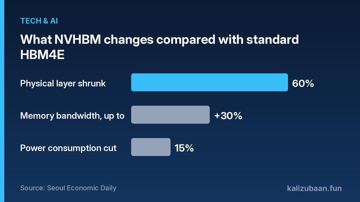
That frees space on the GPU for more computing circuits. To fit the controller, the physical layer that talks to outside chips was shrunk by 60% compared with standard HBM.
Source: Seoul Economic Daily
The result, per the Seoul Economic Daily, is up to 30% more memory bandwidth and 15% lower power use than standard HBM4E, the seventh generation. NVHBM is based on the HBM4E architecture.
Why TSMC, and not Samsung's own foundry
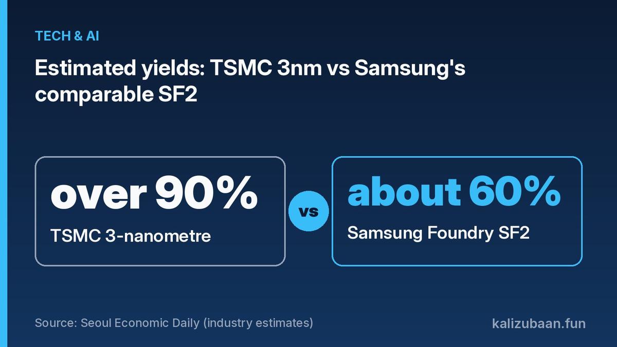
Packing GPU functions onto a small base die needs an ultra-fine process. Keeping costs down also needs high yield, which is the share of working chips on each wafer.
Source: Seoul Economic Daily (industry estimates)
The industry estimates TSMC's 3-nanometre yield at more than 90%, against roughly 60% for Samsung Foundry's comparable 2-nanometre SF2 process. For Nvidia, putting base die production at TSMC is the stable choice.
Nvidia also has a practical reason. When every supplier builds HBM differently, one design can't deliver consistent performance, and each supplier's chips need separate validation. One shared process cuts that burden.
The real driver: not enough memory to go around
Capacity matters as much as technology. Samsung's 4-nanometre base die lines sit only at Hwaseong Line 17 and part of the Pyeongtaek P3 plant. That setup was built for existing HBM demand, not extra custom volumes like NVHBM.
TSMC can fill the gap. At its third-quarter earnings briefing, it said it would add two new 3-nanometre production lines at Fab 18 in Tainan. It also plans 3-nanometre lines in Arizona and Kumamoto, Japan, with the Japan line targeting mass production in 2028.
Samsung isn't giving up its own path. It will keep its turnkey model for standard HBM and for custom HBM for other customers, including AMD. It is also checking whether its own foundry could make NVHBM base dies if demand exceeds TSMC's capacity.
What it means for Indian buyers
You won't buy an HBM chip. But the AI memory rush reaches your phone and laptop.
Wikipedia, quoting industry data, says general DRAM and flash prices saw compounded increases, some exceeding 200%, since early 2025, because of AI demand. Micron has noted a 3-to-1 conversion ratio between HBM and DDR5 wafer capacity, so every HBM ramp squeezes regular memory supply.
You can see it in Indian launches. Beebom describes phone prices as skyrocketing due to the RAM crisis. Samsung's new Galaxy F70 5G starts at Rs 19,999 with just 4GB of RAM.
My take: if you are planning a phone or laptop upgrade, don't wait for memory prices to fall. A deal that fixes supply at Nvidia's scale takes time, and TSMC's new lines only start mass production in the first half of next year.
For students and developers, there is a second lesson. AI performance is now limited as much by memory as by the GPU, which is why memory and chip packaging are becoming some of the most important skills in hardware.
FAQs
What is HBM? High Bandwidth Memory is stacked DRAM placed close to a processor. It is used mainly in AI accelerators, GPUs and data centres because it moves data much faster than regular memory.
What is a base die? It is the logic chip at the bottom of an HBM stack. It controls data transfer speed, and in NVHBM it also holds Nvidia's memory controller.
Is Samsung moving its memory business to TSMC? No. The report says Samsung will use TSMC only for NVHBM base dies at Nvidia's request, and will keep its own process for standard HBM and other customers.
Will this make phones cheaper in India? Not soon. More base die capacity eases one AI bottleneck, but the wider memory shortage is still pushing device prices up.
Sources
- The Economic Times: Samsung to use TSMC technology for Nvidia's next-generation memory chips
- Business Standard: Samsung to tap TSMC technology for Nvidia's custom memory chips
- Seoul Economic Daily: Samsung to tap TSMC for Nvidia's custom HBM base die
- Seoul Economic Daily: Samsung, TSMC join forces to expand custom HBM output for Nvidia
- Wikipedia: High Bandwidth Memory
- Beebom Gadgets: Samsung Galaxy F70 5G goes official in India
Tagged Topics
Keep reading



Thanks for reading Kali Zubaan
Explore more articles in Tech & AI or return to the main publication feed.